
Automotive VCU validation
Development of a Compact Hardware-in-the-Loop Platform
Development of a compact, cost-effective HiL platform designed to enable engineers to validate VCU software in parallel from their own workstations.
IN PROGRESS
Role
Electronics Hardware Engineer
Company
Renco GmbH — Germany
Period
March 2026 - Present
Problem
The company needed a faster and more automated way to validate embedded software on its VCUs. Several employees may need to test VCU software at the same time, and sharing one validation system creates waiting time and limits parallel development. The long-term objective is therefore to provide one validation platform per employee.
Commercial Hardware-in-the-Loop systems provide the required functionality, but purchasing several systems is not financially realistic. In addition to the hardware cost, these systems generally require dedicated software licences. The company therefore needed an internal platform that covers its three main VCUs without requiring a hardware modification when switching between test configurations.
Core requirements
- Cost-effective enough to deploy at multiple employee workstations.
- Compact, easy to transport by hand, and simple to install and operate.
- Suitable for fast and automated embedded-software validation.
- Compatible with the electrical and communication requirements of the company's three main VCUs.
- Configurable through CAN, LIN, Ethernet, or USART without manual hardware changes.
- Powered from the grid without requiring an external laboratory supply.
- Extendable so additional functions and interfaces can be added later.
Solution
I developed a compact Hardware-in-the-Loop platform designed for individual use at an engineer's workstation. It can be transported by hand, installed directly on a desk, and fully configured through software.
The system is designed to cover all the I/O and functions of the company's three VCUs, with additional capacity for external devices such as sensors and other ECUs.
The objective is to deploy identical units across the engineering team so employees can develop and validate VCU software in parallel without the delays, cost, and licensing constraints associated with multiple commercial HiL systems.
Platform capabilities
- Enough analog and digital I/O channels to fully cover the company's three VCUs.
- PWM signal generation and measurement.
- CAN, CAN FD, LIN, Ethernet, SPI, USART, and I²C interfaces.
- Compatible with both 12 V and 24 V systems.
- Software-configurable pull-up and pull-down selection, signal generation, and measurement.
- An extensible architecture that supports additional functions and interface boards.
Method
Step 1 — Requirements definition
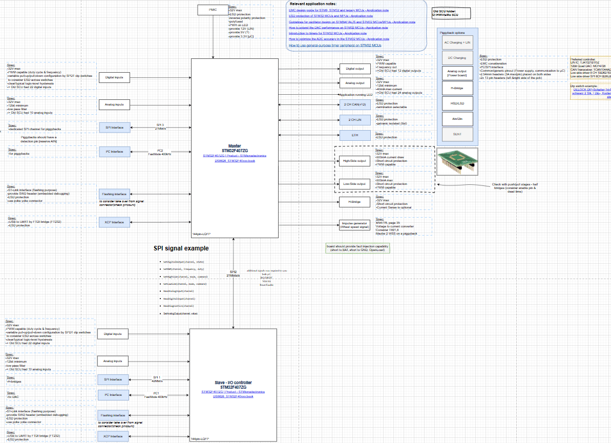
I collected and structured the validation requirements for the company's three target VCUs. This included signal types, channel counts, voltage and current levels, PWM capabilities, communication interfaces, power supply requirements, physical constraints, and future extension needs.
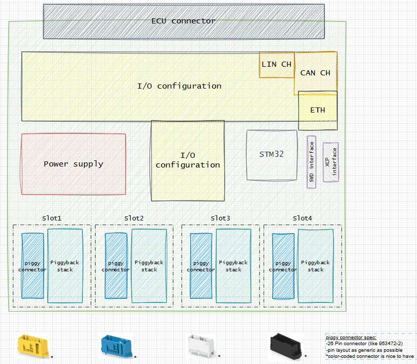
I then created a high-level system diagram in draw.io showing the processing architecture and all required driver blocks, with the requirements for each block documented directly in the diagram.
Step 2 — Driver and microcontroller selection
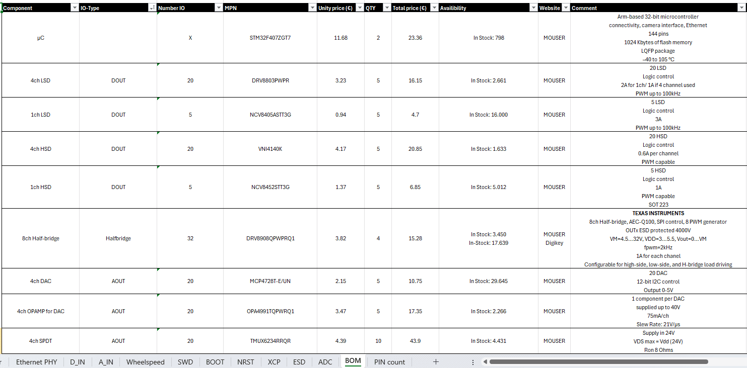
I selected the main components based on the required digital and analog signal channels and their performance requirements, as well as the necessary PWM, timer and communication interfaces, processing performance, electrical specifications, availability, and cost.
A dual-STM32F407ZGT7 architecture was selected because one microcontroller did not provide enough pins, timers, and peripheral resources for the complete system. I selected the principal interface drivers, fixed the first detailed architecture, and prepared a preliminary BOM estimate to verify the cost direction.
Step 3 — Schematic design
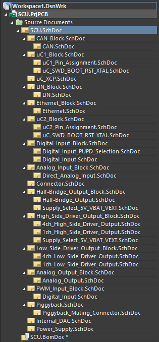
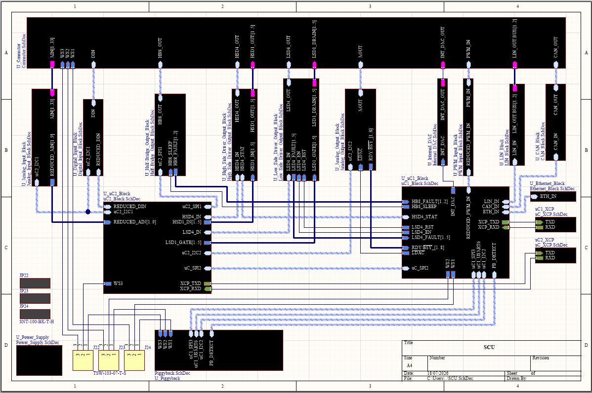
I created the first complete schematic in Altium Designer using the selected microcontrollers, interface drivers, and communication components. Placeholder passive components were initially used around the main drivers so the circuit architecture could be defined before every value and reference was fixed.
I used hierarchical sheets, repeated functional blocks, multi-channel structures, harnesses, buses, reusable circuits, and centralized component-parameter management. I then sized and selected the remaining filters, protection devices, resistors, capacitors, connectors, and supporting components for the complete project.

Step 4 — BOM development and cost control
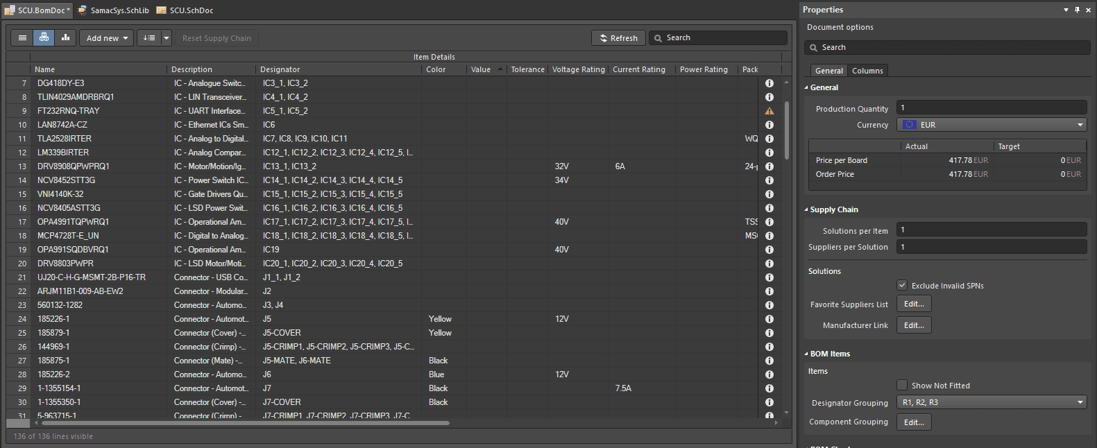
I developed the BOM in parallel with the schematic using Altium ActiveBOM. Each schematic update was reflected in the cost and sourcing view, allowing me to monitor supplier references, component availability, alternatives, missing parameters, individual component prices, and the resulting total hardware cost.
This continuous process reduces the risk of discovering expensive or unavailable components after the schematic is complete. The BOM remains preliminary and will be finalized after the ongoing circuit validation.
Step 5 — Prototyping and experimental validation
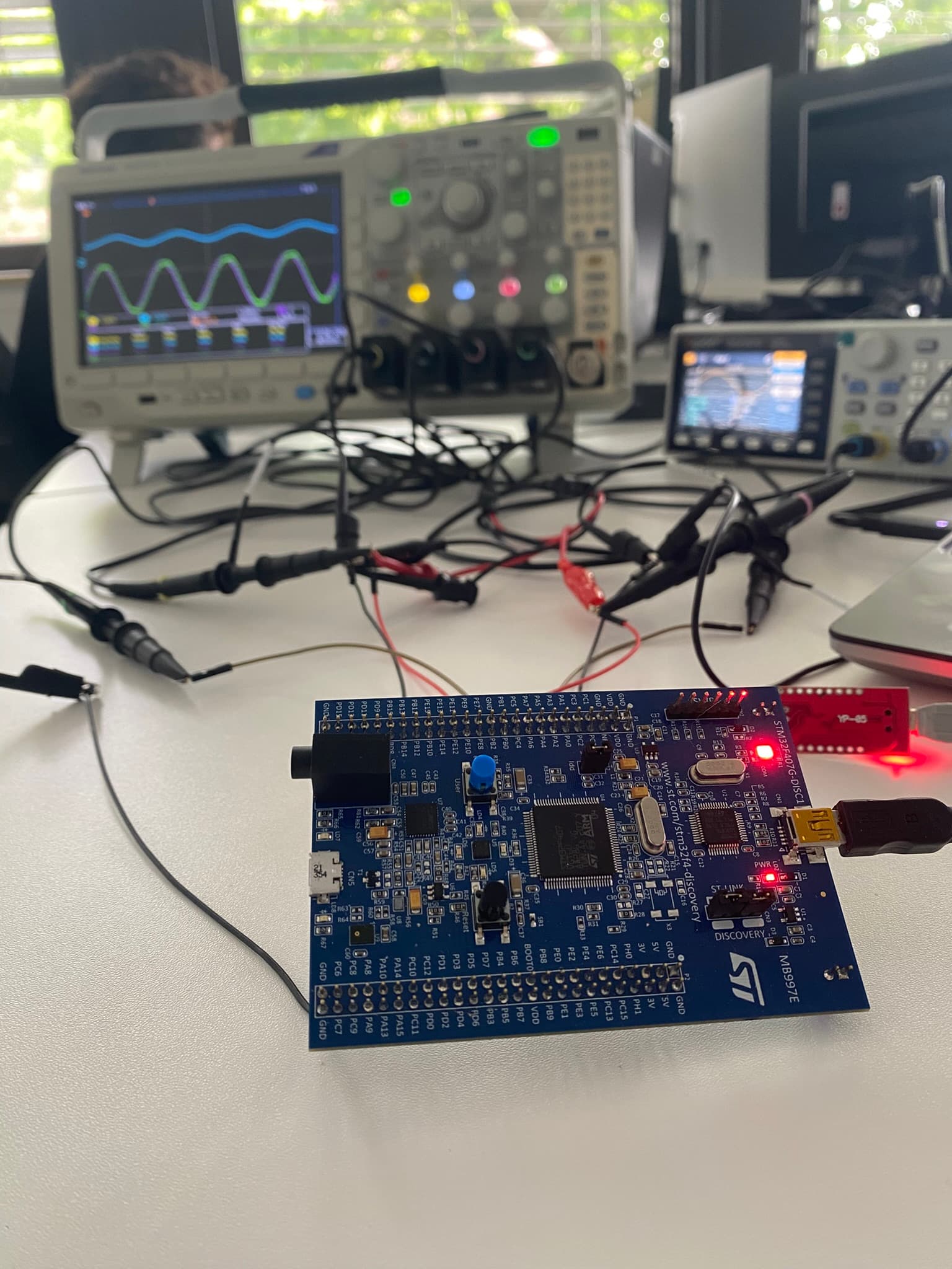
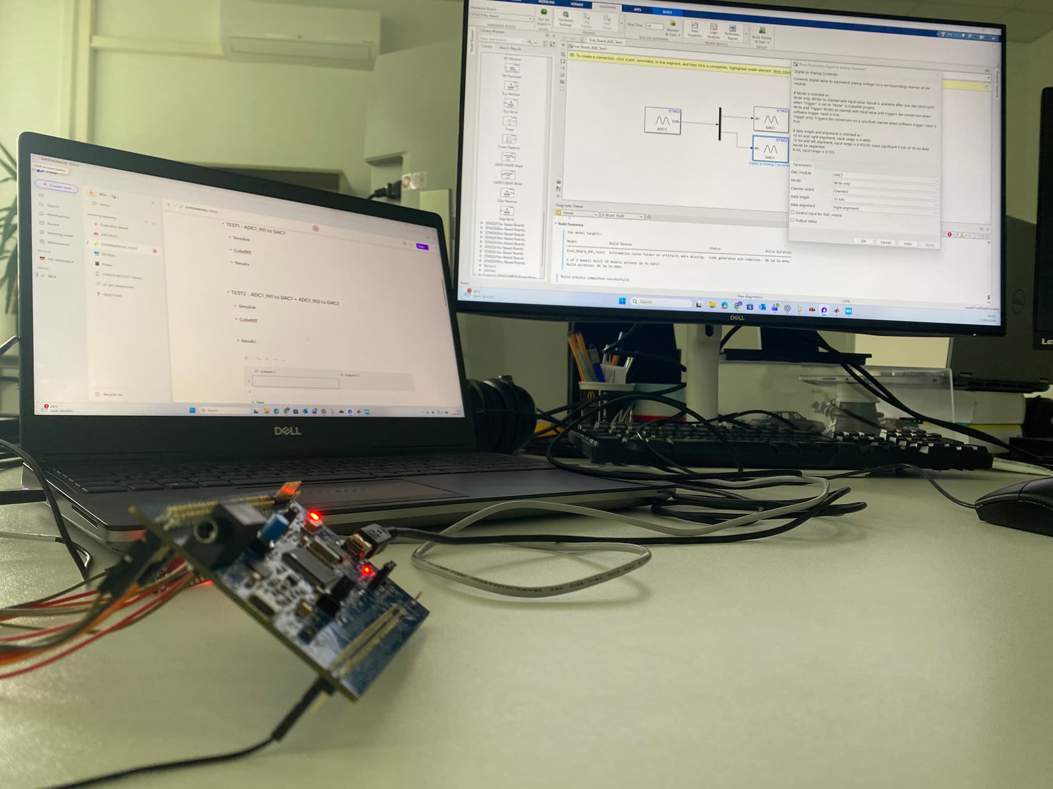
The project is currently in the prototyping phase. Using one STM32F407G-DISC1 evaluation board, I have tested the microcontroller’s digital and analog I/O, PWM generation and measurement, timer resources, timing precision, GPIO speed, and peripheral behavior.
Communication and resource coordination between the two microcontrollers have not yet been tested. Validation of the interface drivers, signal-conditioning stages, protection circuits, and other representative circuit sections will be performed in the next phase. The purpose is to identify limitations before PCB layout and manufacturing, while corrections can still be made at schematic level.
Results
The project has progressed from requirements definition to a complete first schematic-level architecture. The final PCB has not yet been manufactured; current tests are being used to confirm the critical design assumptions before the schematic is frozen.
Completed at this stage
System definition and architecture
- Requirements defined for the company's three main VCUs, including channel counts, electrical levels, communication interfaces, power, and physical constraints.
- High-level system architecture and dual-STM32F407ZGT7 processing architecture established.
- I/O architecture completed for 66 analog channels—33 inputs and 33 outputs—and 116 digital and power I/O channels—50 digital inputs, 25 high-side outputs, 25 low-side outputs, and 16 half-bridge outputs.
- PWM capability allocated across 44 channels up to 2 kHz: 14 PWM inputs and 30 PWM outputs.
- Two CAN/CAN FD interfaces with switchable termination, two LIN interfaces, Ethernet, SPI, USART, and I²C.
Detailed hardware design
- 12 V and 24 V-compatible signal conditioning, configurable pull-up and pull-down functions, and protection circuits designed.
- Complete hierarchical schematic created in Altium Designer using reusable and repeated functional blocks.
- Nearly all components selected and sized, including all resistors and capacitors; the remaining revisions will be driven by circuit-validation results.
Engineering readiness and validation
- Preliminary BOM, sourcing review, and cost estimate prepared.
- MCU pin, timer, and peripheral allocation prepared in STM32CubeMX.
- Initial MCU-level validation completed for analog and digital I/O, PWM generation and measurement, timer resources, timing precision, GPIO speed, and peripheral behavior.
Next Steps
The remaining work will progress from targeted prototyping of critical circuitry and schematic refinement to PCB layout, manufacturing, board bring-up, and validation of functionality and accuracy against a defined test plan covering the company's three target VCUs.
1. Prototype and validate critical circuitry
- Prototype every circuit identified during the design phase as requiring experimental validation.
- Focus testing on complex or performance-critical circuits where functionality, accuracy, or component behavior cannot be confirmed through analysis alone.
- Measure performance under representative operating conditions.
- Update the schematic and component values according to the test results.
2. Complete the PCB layout and design review
- Begin the PCB layout after incorporating the prototyping results and finalizing the schematic.
- Define the placement and routing while considering controlled impedance, parasitic track capacitance, signal integrity, grounding, current capacity, and thermal constraints.
- Use AI-assisted checks to support the design-review process alongside standard engineering verification.
3. Finalize manufacturing data and prepare the test plan
- Complete the PCB design, manufacturing files, assembly data, and final BOM.
- Order the PCB and components.
- Develop a detailed board bring-up and validation plan in parallel with PCB manufacturing and component procurement.
- Define the required equipment, test sequence, expected results, tolerances, and acceptance criteria.
4. Assemble, bring up, and validate the board
- Assemble the PCB and perform a controlled initial bring-up.
- Test the board against the validation plan.
- Verify the functionality, accuracy, timing, communication interfaces, protection circuits, and repeatability of the complete system.
- Document the results and correct any issues identified before approving the design.